HMT-Global SiC Wafer Manufacturers & Suppliers

Raw-cut SiC Wafer (Unpolished)
PRODUCT PARAMETERS
Description
As a Raw-cut SiC Wafer Manufacturer, HMT can make and customize any thickness SiC Wafer (DSP) and Raw-cut SiC Wafer (Unpolished). Like: 800um 900um 1100um 1200um 1500um etc. Unpolished SiC Wafer dimension from 2” 4” to 6” 8” all available in HMT company. Even for special customized SiC wafers, we still offer the great price for our customers. Don’t hesistate to contact us, customize your needs today!
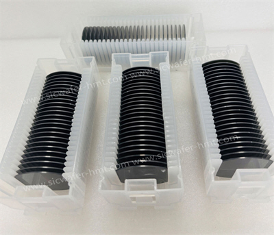
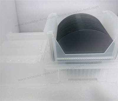
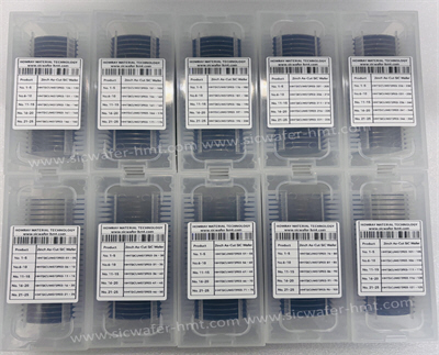
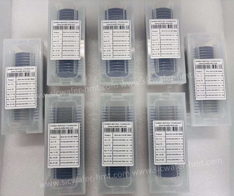
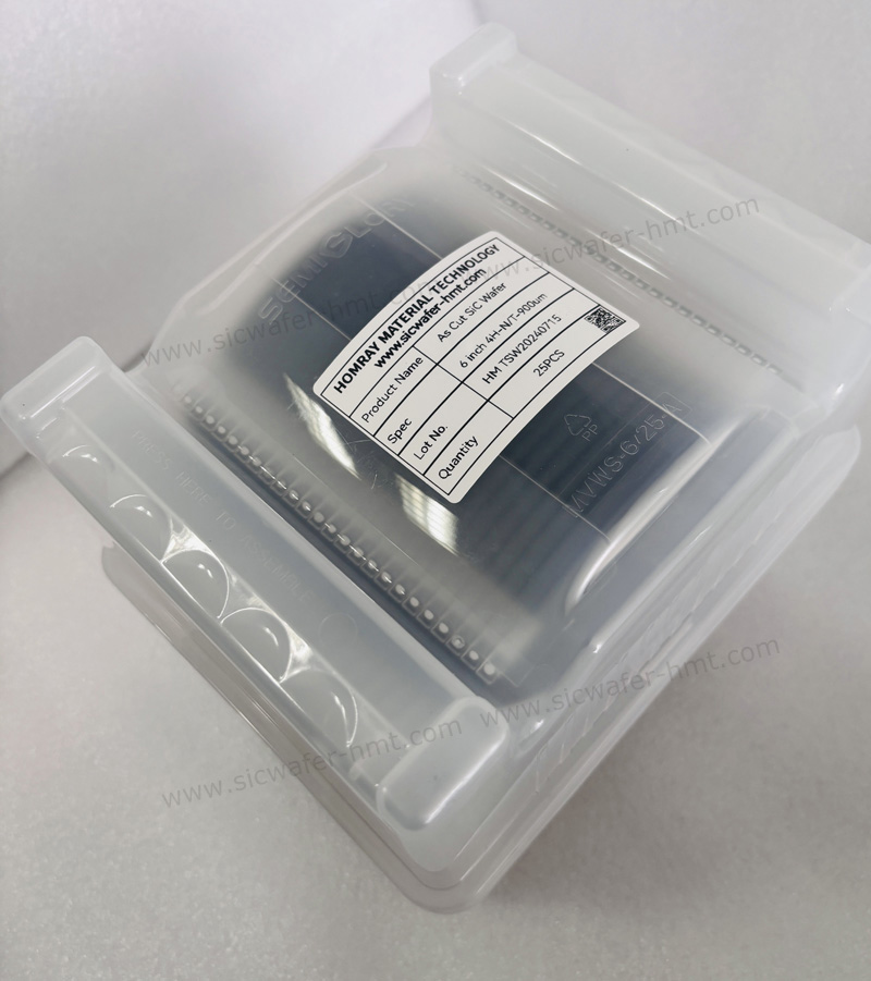
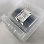
2 inch and 6 inch Raw-cut SiC Wafer Pictures
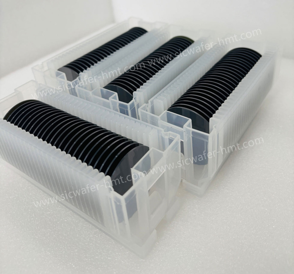

Raw-cut SiC Wafer For CMP Testing Application
The typical SiC crystal processing flow primarily consists of three key steps: slicing, grinding, and polishing. Slicing, as the first step, plays a critical role in determining the quality of subsequent grinding and polishing processes. Key parameters such as bow, warp, and total thickness variation (TTV) of the sliced wafers are decisive for follow-up operations. The purpose of grinding is to remove saw marks and surface damage caused during slicing. As well as to correct deformation introduced by the cutting process. Due to the high hardness of SiC, high-abrasive materials such as boron carbide or diamond powder must be used to grind the surface of sliced SiC wafers.
Polishing is employed to enhance the surface finish and flatness of the wafers, primarily through chemical mechanical polishing (CMP). This process combines chemical etching and mechanical wear to achieve global planarization of the wafer surface. Customer can purchase unpolished wafer from HMT company for CMP testing with very low cost.
To fully leverage the effectiveness of CMP polishing for SiC wafers, precise coordination between process parameters and polishing materials is essential. Key factors include the chemical composition of the polishing slurry. The physical characteristics of the polishing pad (such as hardness and porosity). The selection of abrasive particles (e.g., silica, ceria), and their synergistic interactions.