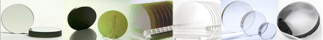
HMT-Global SiC Wafer Manufacturers & Suppliers

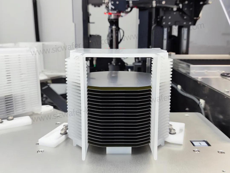
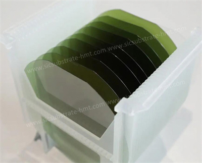
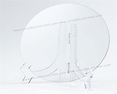
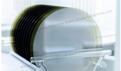
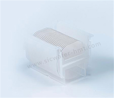
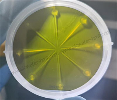
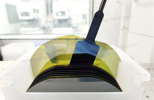
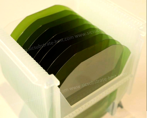
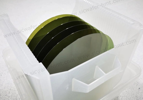
6 inch 4H-N SiC Wafer

PRODUCT PARAMETERS
Description
HMT is a semicondutor company that manufactures 6 inch 4H-N SiC Wafer (150mm). Actually,HMT can customize and produce any thickness 4H-N type SiC wafer SiC raw cut wafer like normal thickness 350um or 500um,800um. Even you choose customize wafers, you can still get the preferential price and professional services. Available size of SiC Wafer: 2” 4” 6” 8” and largest 12”. With our rich experience and knowledge in the wafer industry, you can be confident in making HMT your first choice.
- Basic Spec
- Diameter: 150±0.25mm
- Thickness: 350um, Customize 500um,800um
- Grade: Production Grade
- Dopant: Nitrogen
- Orientation: 4°toward<11-20>±0.5º
- Resistivity: 0.015-0.028 ohm.cm
- Micropipe density: ≤0.2ea/cm²
- Surface finish: Si face CMP, C face polished
N-type SiC Wafer Advantages
N-type SiC Wafer refers to a silicon carbide monocrystalline wafer manufactured by doping with specific impurity elements such as nitrogen (N). N-type SiC substrates offer advantages such as high electron mobility, high free electron concentration, and excellent high-temperature stability, making them highly sought-after in fields like radio frequency communication, electronic and electrical applications, and optoelectronic devices.
Silicon carbide (SiC) is the primary raw material for N-type silicon carbide substrates, accounting for a significant portion of their production costs. Silicon carbide exhibits properties such as resistance to high frequencies, high temperatures, and high voltages, making it widely applicable across various domains.
Silicon carbide substrate refers to a single-piece material primarily made from silicon carbide powder through manufacturing processes such as crystal growth (where overcoming lattice defects and controlling crystal forms are key), ingot processing, cutting, grinding, polishing, and cleaning. It serves as the foundational material for producing wide-bandgap semiconductors and other silicon carbide-based devices, offering significant advantages in high-frequency and high-voltage applications such as new energy vehicle electronic controls, photovoltaic inverters, and 5G base stations.