HMT-Global SiC Wafer Manufacturers & Suppliers

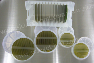
4H-Silicon Carbide(SiC) Substrate CMP
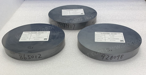
PRODUCT PARAMETERS
Description
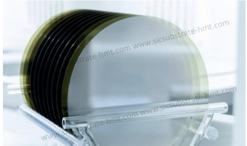
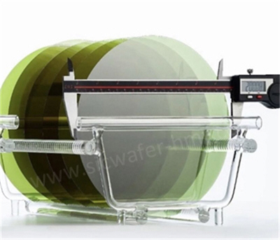
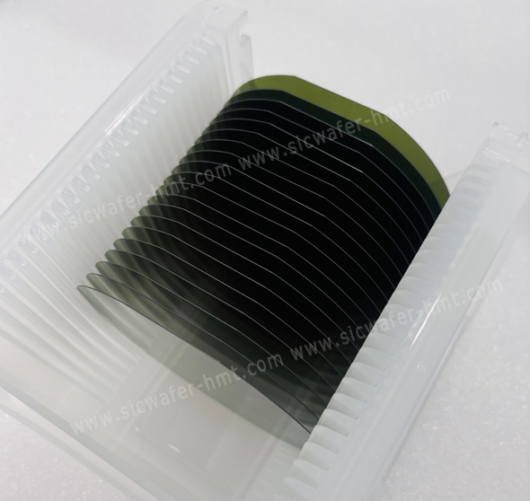
The transformation of a silicon carbide (SiC) substrate—from a gray ingot with hardness second only to diamond, to a mirror-smooth surface that reflects one’s image—is a vivid testament to the power of human precision manufacturing against material limits. This journey is also the core domain where leading 4H-Silicon Carbide(SiC) Substrate Suppliers worldwide continuously push the boundaries of technology. HMT can offer SiC substrate from 2 inch to 8 inch, including 4H-N,4H-P and 4H-SI type for power electronic and optic ARAI applications.
However, you may not know that silicon carbide, hailed as the core material of the “third-generation semiconductors,” possesses such extreme hardness that almost only diamond can rival it.
Processing such a “tough nut” into a near-perfect mirror-like substrate presents a challenge several times greater than that of traditional silicon materials. This is not only a core challenge in semiconductor manufacturing but also a key factor determining device performance and cost.
4H-Silicon Carbide(SiC) Substrate Processing Flow
The processing of SiC substrates is a precision system engineering journey from macroscopic shaping to atomic-level flatness. Its core objective is to transform rough slices cut from an ingot into a flawless “foundation” with surface roughness below 0.3 nanometers and free of subsurface damage, ready for the subsequent epitaxial growth of high-quality semiconductor device structures.
The entire process follows a logic of “first shape, then refine, finally perfect,” primarily consisting of three core steps: slicing, grinding, and polishing.
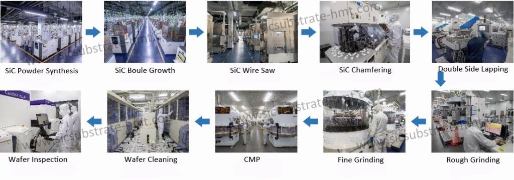
Key Processes in SiC Substrate Manufacturing
As the first step, the quality of slicing determines the starting point for all subsequent processes. The core challenge is to slice wafers as thin as possible to improve yield per ingot, while simultaneously avoiding breakage, warping, and deep-layer damage caused by the material’s high hardness and brittleness. Slicing is key to determining material utilization and the starting point for processing. As wafer size progresses from 6 inches to 8 inches and larger, traditional diamond inner/outer diameter saws are being phased out due to their wide kerf, poor surface quality, and high noise.
Japan’s DISCO company’s KABRA Stealth Dicing technology and Infineon’s acquired “Cold Split” technology have garnered significant attention. These technologies use lasers to create modified layers or micro-cracks inside the crystal, followed by mechanical separation. They can control the total kerf loss per wafer to within 100 micrometers, theoretically improving material utilization by nearly threefold.
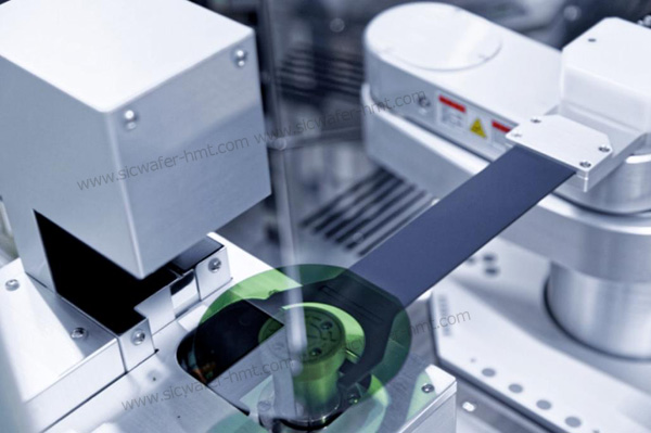
Lapping and Polishing
The wafer surface after slicing has deep damage and severe deformation, requiring grinding to rapidly remove the damaged layer and correct geometric shape. Based on the processing principle and purpose, grinding is divided into coarse grinding and fine grinding.
The task of coarse grinding is to remove material quickly and in large volumes, using coarser diamond abrasives. It can correct the wafer’s Total Thickness Variation (TTV) to 3-5 micrometers and reduce surface roughness (Ra) to 20-30 nanometers within minutes. Fine grinding uses finer abrasives, aiming to create a near-perfect precursor surface for subsequent polishing, controlling TTV below 2 micrometers and roughness (Ra) to 1-2 nanometers.
Polishing, especially Chemical Mechanical Polishing (CMP), is the decisive step to obtain the final “mirror” surface. Its goal is to completely eliminate all mechanical damage, achieving an atomically smooth (Ra < 0.3 nm), ultra-clean surface free of subsurface damage.
Pure mechanical polishing can reduce roughness but is prone to introducing scratches, while pure chemical polishing is inefficient due to the chemical inertness of SiC. CMP ingeniously combines chemical etching and mechanical abrasion: chemical agents in the polishing slurry first react with the SiC surface to form a softer oxide film, which is then gently removed by mechanical action.