HMT-Global SiC Wafer Manufacturers & Suppliers

About Us

Who We Are
We are the professinal & reliable
SiC Wafer SiC Boule Manufacturer
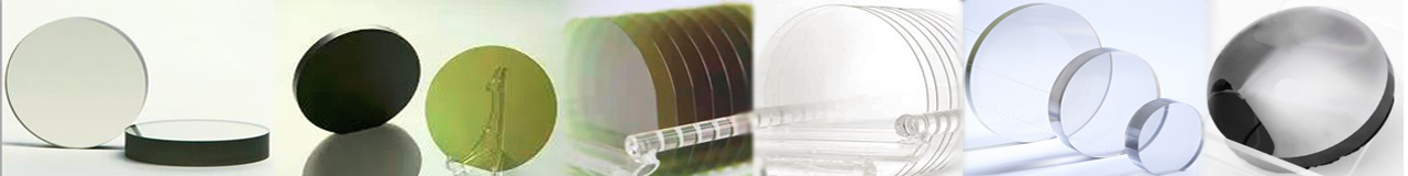
Homray Material Technology(HMT) was established in 2009, is a professional manufacturer and supplier of SiC Wafer/SiC Substrate ( 4H-N Conductive Type), As-cut SiC Wafer/SiC Unpolished Wafer (4H-SI/Semi-insulating Type), SiC Boule/Ingots and SiC Epi Wafer. SiC Wafer dimension including 8 inch, 6 inch, 4 inch, 2 inch. SiC Wafer Grade including P(Production) Grade , R(Research) Grade, D(Dummy) Grade. Different SiC Wafer thickness like 350um, 400um, 500um, 600um, 900um,1000um, 1100um, 1200um all can be customized. It is widely acknowledged that compound Semiconductor (SiC,GaN) with its superior property like wide-bandgap, is expected to the most promising material choice for next generation device. SiC device/module can achieve low loss and fast switching/oscillation simultaneously because of its high critical electrical field.
Homray Material Technology is committed manufacturing excellent quality SiC Boule Ingot, SiC Wafer/SiC Substrate and SiC Epi Wafer for SiC MOSFET, SiC SBD, and SiC RF HEMT, Power HEMT electronics and opto-electronics applications. As the leading SiC Boule and SiC Wafer manufacturer and supplier in the compound semiconductor industry, our dealers and partners are mainly distributed in Europe, USA, Southeast Asia, and South America, our annual revenue exceeded 78 Million US dollars in 2023. Excellent products quality and professional service won the trust and support from our customers in the world.
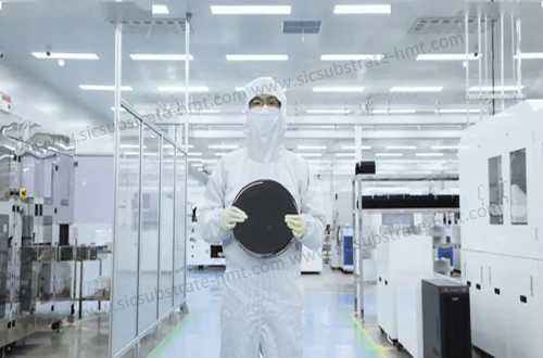
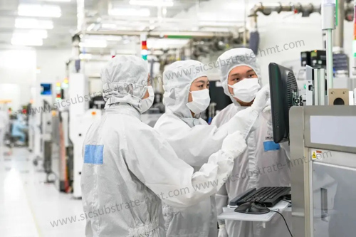
Our Manufacturing
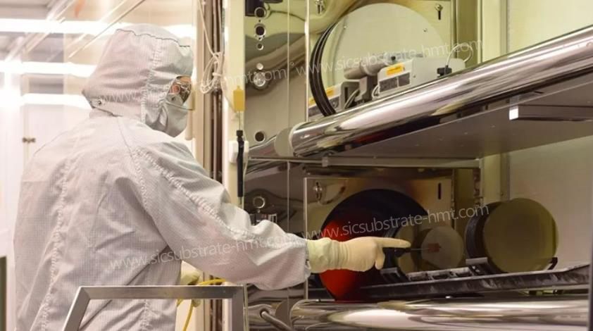
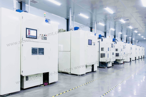
Wafer Fab Facility
As a global SiC Wafer Manufacturer and Supplier, HMT use PVT method growing SiC Boules. This method need to sublimate the powder with high temperature and vacuum, and let the components grow on the seed surface through thermal filed control, so as to obtain the SiC crystals. Before shippment, we will cleaning wafer and inspeciton SiC Wafer. We use safe Cassette to package all SiC Wafers.
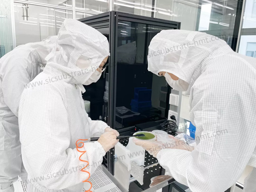
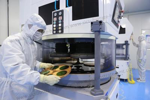
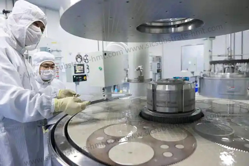
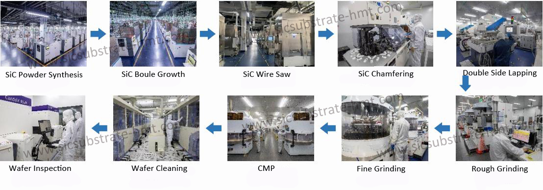
Our Process
SiC Wafer Process
As the reliable SiC Wafer, SiC Substrate, SiC Boule Manufacturers and Suppliers, HMT company has established whole SiC Substrate Wafer production line. Using Physical Vapor Transfer (PVT) method formation SiC Boule, then SiC Boule through SiC Wire Saw, SiC Chamfering, SiC Wafer Lapping, SiC Wafer Grinding, SiC Wafer Polishing/CMP, SiC Wafer Cleaning & Inspection etc steps to produce the high quality SiC Substrate Wafers.