HMT-Global SiC Wafer Manufacturers & Suppliers

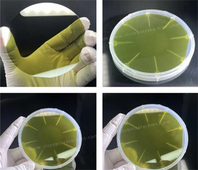
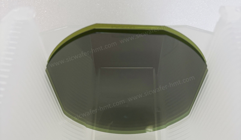
P Type SiC Epi Wafer
PRODUCT PARAMETERS
Description
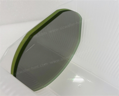
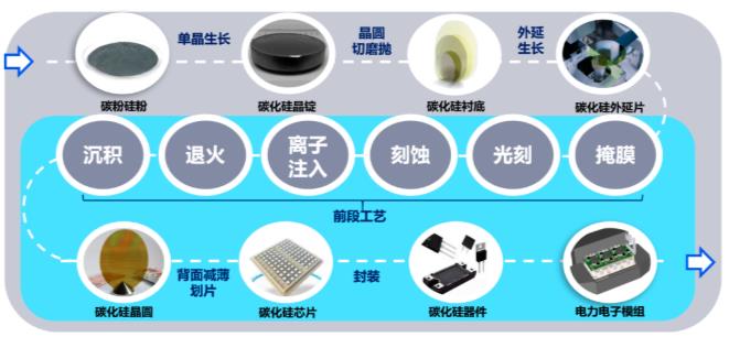
As a leading SiC Epi Wafer Manufacturer, we supply high-quality n-type and p-type epitaxial wafers on 4 inch, 6 inch, and 8 inch substrates to meet diverse application needs. Epitaxial growth is a core process in the production of SiC devices, accounting for approximately 22% of the total manufacturing cost. It is a critical step that directly determines the performance of the final chip.
HMT SiC Epi Wafer Spec
- Dimension: 4inch, 6inch,8inch
- Substrate: Silicon Carbide SiC
- Substrate Grade: Production
- Substrate Thickness: 350±25um/ 500±25um
- Epi Layer Dopant: Aluminum or Nitrogen
- Thickness:0.2~100um
- Bufffer : N type 1μm1E18cm-3
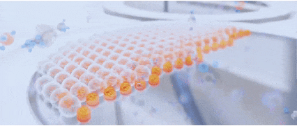
Epitaxial growth involves using precisely controlled chemical reactions to “grow” a uniform layer of silicon carbide film on the surface of this SiC substrate. This layer is called the “epitaxial layer.”
The epitaxial layer is not grown arbitrarily; it is custom-designed according to the specific performance requirements of the chip. How is this achieved? This leads us to a core thin-film fabrication technology in the semiconductor field: Chemical Vapor Deposition (CVD).
SiC epitaxial growth is accomplished via high-temperature CVD. After precursor gases are activated by high temperatures, the resulting products deposit to form a thin film. The process can be broadly divided into three steps:
Step 1: Preparing a Clean Environment
The polished SiC substrate is placed into a specialized epitaxial growth reactor. The chamber is evacuated to a near-perfect vacuum to avoid contamination, and an inert gas (such as argon) is introduced for protection. The temperature is then raised to between 1600°C and 1700°C – a range high enough to facilitate the necessary chemical reactions without damaging the substrate’s crystal structure.
Step 2: Precise Delivery of Reaction Precursors
Using a precisely controlled gas delivery system, three core types of precursor gases are introduced into the reactor:
- Gases carrying silicon, such as trichlorosilane (HSiCl₃).
- Gases carrying carbon, such as propane (C₃H₈).
- Dopant gases used to tailor electrical properties, such as nitrogen (N₂) for n-type doping or an aluminum source for p-type doping.
Step 3: Directed Film Growth
In the high-temperature environment, the precursor gases undergo chemical reactions on the substrate surface, decomposing into silicon and carbon atoms. These atoms arrange themselves according to the crystal structure of the substrate, gradually building up layer by layer to form a thin film. The result is an exceptionally smooth and uniform epitaxial layer. The thickness of this layer is increased accordingly for chips requiring higher voltage resistance.
After the epitaxial growth process, the combined structure of the substrate and the epitaxial layer is called an “epitaxial wafer.” This now provides a flat and suitable “processing foundation” ready for subsequent circuit fabrication steps such as photolithography and etching.