HMT-Global SiC Wafer Manufacturers & Suppliers

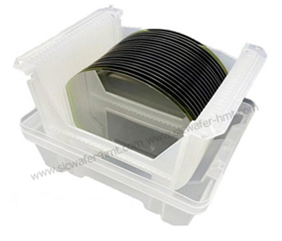
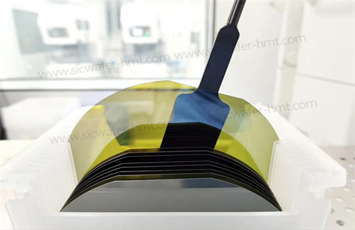
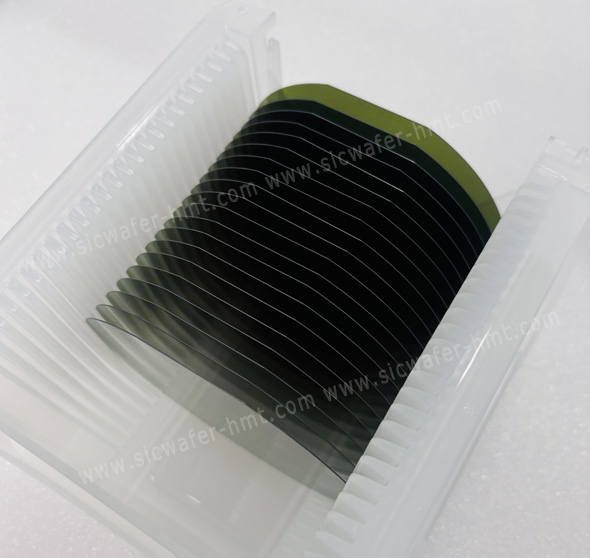
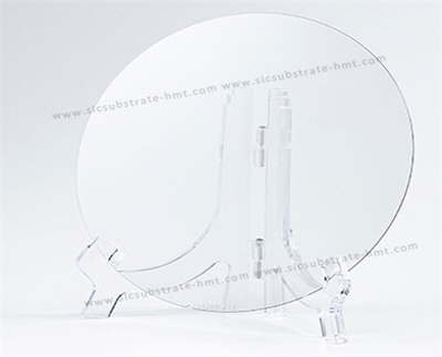
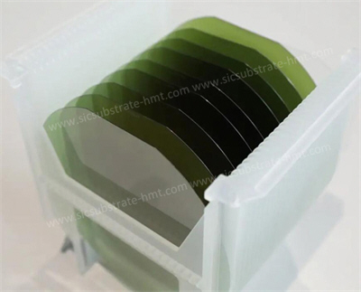
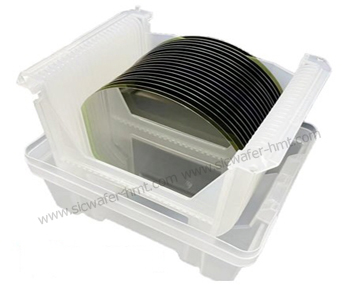
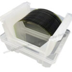
8 inch SiC Wafer D Grade


PRODUCT PARAMETERS
Description
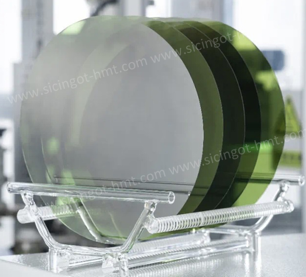
HMT SiC Wafer Player and Maker is a company that manufactures and supplies 8 inch SiC Wafer (polished), As-cut SiC Wafers (unpolished) and related SiC products. HMT manufactures 4H n type SiC Wafer with Nitrogen doped and un- doped. Available size from 2’’ to 8’’ which is dummy or production grade for the electronics and optoelectronics industries. HMT can make and customize any thickness SiC wafer SiC raw cut wafer like 600um 800um 900um 1100um etc. with great price at the market. Please contact us today to discuss your project requirements.
8 inch SiC Wafer(Thickness 500um)
SiC Wafer refer to single-piece materials made primarily from SiC powder through a series of manufacturing processes, including crystal growth (where overcoming lattice defects and controlling crystal forms are key), ingot processing, cutting, grinding, polishing, and cleaning. These wafers serve as the foundational material for producing wide-bandgap semiconductors and other SiC-based devices, offering significant advantages in high-frequency and high-voltage applications such as new energy vehicle electronic controls, photovoltaic inverters, and 5G base stations.
- 8 inch SiC Wafer Basic Spec
- Grade: D Grade
- Diameter: 200±0.5mm
- Thickness: 500±25um
- Orientation: off axis 4.0° toward<11-20>±0.5°
- Micropipe density: ≤1 ea/cm²
- Surface finish: Si-face CMP, C-face polished
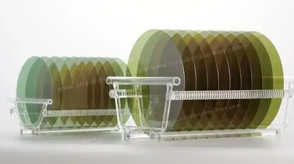
The 6‘’ conductive SiC substrate remains the mainstream in the market (due to its mature technology, relatively controllable costs, and compatibility with most current silicon carbide device production lines). The demand for 8‘’ conductive substrates is gradually rising (aligning with the trend of large-size wafer manufacturing, improving chip production efficiency and cost advantages). Meanwhile, 12 inch conductive substrates have already seen research samples (addressing challenges in large-size crystal growth and processing yield, which will pave the way for higher-end applications).