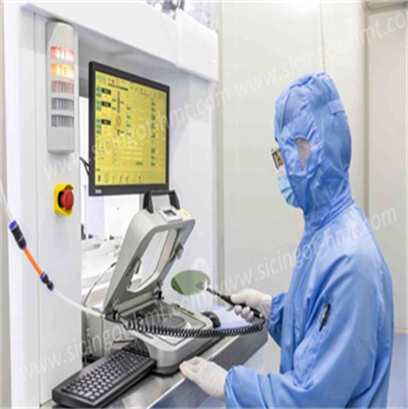
HMT-Global SiC Wafer Manufacturers & Suppliers

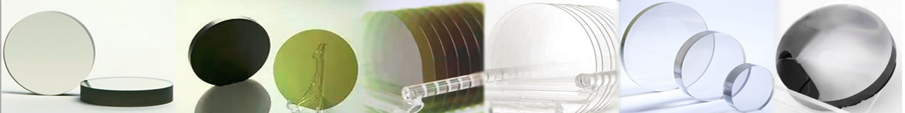
Types of Wafer Substrates
In semiconductor manufacturing, wafer substrates serve as the physical foundation for chip devices and directly impact chip performance, power consumption, and reliability. Let SiC Substrate Manufacturer HMT introduce of different application substrate materials can be broadly categorized into the following types:
Silicon (Si)
Silicon dominates over 95% of the global semiconductor market, making it the most widely used substrate material. Its core advantages include low cost (abundant silicon dioxide raw materials), mature manufacturing processes (supporting advanced nodes like 3nm). And the ability to produce large-diameter wafers with stable mechanical properties that facilitate cutting and polishing.
Gallium Arsenide (GaAs)
Gallium arsenide is primarily used in high-frequency radio frequency (RF) devices (e.g., 5G/6G front-end modules) and optoelectronic devices (e.g., lasers, infrared light sources). Its electron mobility is 5–6 times higher than that of silicon, making it ideal for high-speed communication applications. Its direct bandgap (1.42 eV) enables efficient photoelectric conversion, making it a foundational material for infrared lasers and LEDs. It also exhibits high resistance to heat and radiation, making it suitable for aerospace applications.
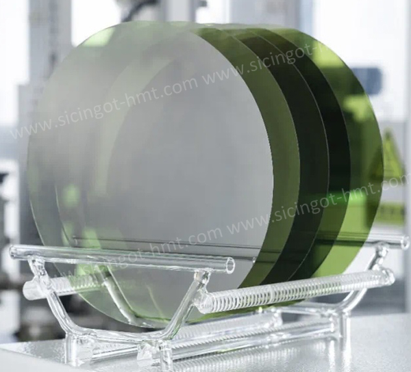
Silicon Carbide(SiC)
Silicon carbide is tailored for high-voltage and high-temperature applications, such as electric vehicle inverters, industrial power supplies, and aerospace equipment. Its wide bandgap (3.26 eV) enables it to withstand breakdown voltages ten times higher than silicon. Operate at temperatures exceeding 200°C. And exhibit thermal conductivity three times that of silicon, resulting in excellent heat dissipation. These properties significantly enhance system power density and energy conversion efficiency.
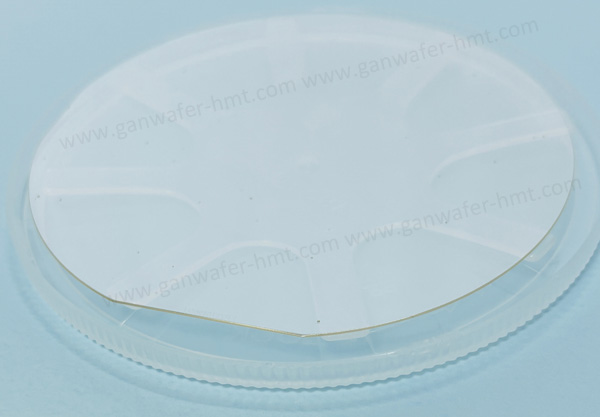
Gallium Nitride (GaN)
Gallium nitride is widely used in fast chargers, 5G base station RF components, and blue LEDs. Its wide bandgap (3.4 eV) combines high-frequency (>100 GHz) and high-voltage capabilities, with low on-resistance reducing energy loss. It is often grown heteroepitaxially on silicon, sapphire, or SiC substrates to lower costs.
Sapphire (Al₂O₃) and Ceramic Substrates
Sapphire is a critical substrate for LED lighting due to its low cost, chemical stability, and transparency, making it suitable for vertical-structure LED epitaxial growth. However, its lattice mismatch with gallium nitride exceeds 13%, requiring buffer layers and resulting in high defect density. Its low thermal conductivity (approximately 1/20 that of silicon) limits its use in high-power LEDs. Ceramic substrates such as alumina and aluminum nitride are used as heat-dissipating bases for high-power modules, offering both insulation and high thermal conductivity. However, their non-single-crystal structure prevents direct device growth.