HMT-Global SiC Wafer Manufacturers & Suppliers

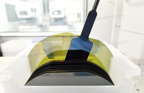
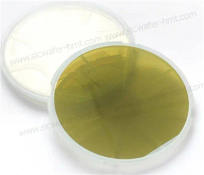
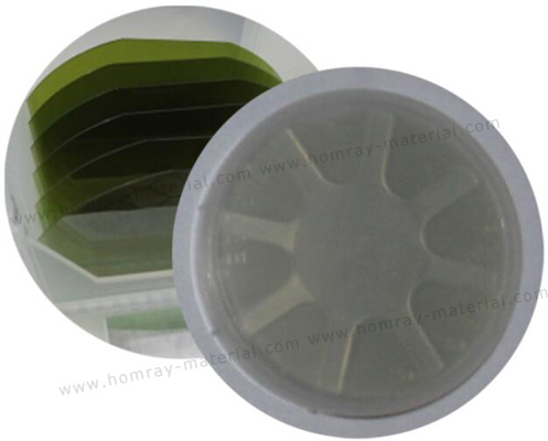
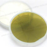
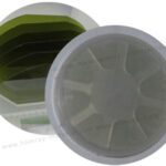
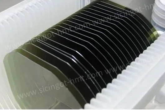
4 inch SiC Wafer
PRODUCT PARAMETERS
Description
Homray Material Technology as the professional 4inch SiC Wafer Supplier, specializes in manufacturing high-performance 2inch 4inch 6inch and 8inch silicon carbide (SiC) wafers, available in Conductive N-type (doped with nitrogen) and semi-insulating (HPSI) types (undoped type). These wafers feature exceptional material properties, including:
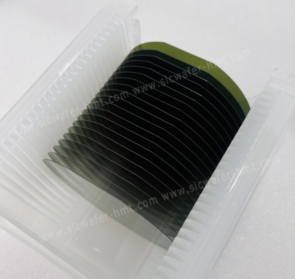
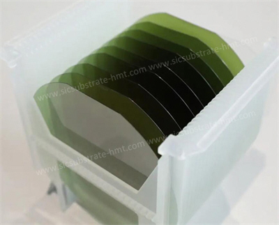
- Dimensions: 350 μm ± 25 μm thickness, on-axis and off-axis orientation .
- Crystal Structure: 4H polytype with low defects, optimized for epitaxial growth.
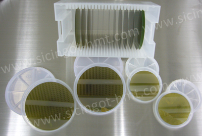
- Cutting Technology: Processed via diamond wire cutting or advanced laser stripping to minimize surface damage (Ra/TTV/BOW control), ensuring superior flatness for downstream processes
| Item | HMT Spec |
| Diameter | 350±25μm |
| Grade | D / R / P |
| Surface orientation | 4° toward <11-20> ± 0.5º |
| Dopant | n-type Nitrogen |
| Micropipe density | ≤ 5 ea/cm 2/ ≤ 1 ea/cm 2 / ≤ 0.5 ea/cm 2 |
| Resistivity | 0.15~0.025ohm·cm |
| Primary flat length | 32.5± 2mm |
| Surface finish | Si-face CMP/C-face polished |
4inch SiC Wafer Applications
- Power Electronics:
Enables high-voltage, high-temperature devices (SBDs, MOSFETs, IGBTs) for electric vehicles, solar inverters, and industrial motor drives, reducing energy loss by up to 70% compared to silicon . - RF & Military Systems:
Semi-insulating wafers serve as substrates for GaN HEMTs in 5G base stations, satellite communications, and next-gen radar systems (e.g., phased array radars), enhancing power density by 10× . - Emerging Hybrid Devices:
Supports monolithic integration of GaN/AlGaN heterostructures on SiC for high-frequency, high-reliability applications, usually used for microwave frequency devices.
Why Choose HMT?
As a certified 4inch SiC wafer supplier based in Suzhou, China, we combine cost efficiency with crystal growth technology. Our wafers align with industry shifts toward larger diameters and higher thermal conductivity needs